Customized Two-Stage Differential Amplifier
Fall 2025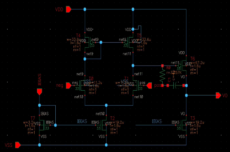
Overview
Designed a two-stage differential amplifier with a tail current mirror, active load, and Miller compensation capacitor. Operating from a 1.5V supply with a 2pF load, the amplifier met or exceeded every design target — including a 76.96 dB voltage gain, 6.91 MHz unity-gain frequency, and only 0.0874 mW of power dissipation. The design process involved full hand calculations for transistor sizing (Gm1 = 175 µA/V, Gm2 ≈ 133 µA/V), followed by HSPICE simulation and iterative refinement in Cadence Virtuoso.
Design Approach
The first stage uses a differential pair with a PMOS current mirror active load to maximize voltage gain. A tail current source sets the bias point and sets the common-mode rejection ratio. Miller compensation between the first and second stage output nodes shifts the dominant pole to a low frequency, ensuring sufficient phase margin at unity gain. Device W/L ratios were derived from hand calculations targeting the specified Gm values and then tuned through simulation to hit the slew rate and CMRR specs simultaneously.
Performance Results
| Specification | Required | Obtained |
|---|---|---|
| Supply Voltage | 1.5 V | 1.5 V |
| Output Swing | > 1.20 V | 1.217 V |
| Voltage Gain | ≥ 75 dB | 76.96 dB |
| Unity-Gain Frequency | ≥ 5 MHz | 6.91 MHz |
| Phase Margin | ≥ 60° | 61.2° |
| Power Dissipation | ≤ 0.1 mW | 0.0874 mW |
| CMRR | > 70 dB | 70.86 dB |
| Slew Rate | > 4 V/µs | 5.65 V/µs |
Full Report
The full report includes all hand calculations, device sizing tables, and HSPICE simulation waveforms.