16-bit SAR ADC Controller
Fall 2025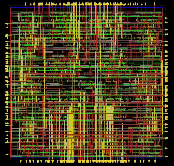
Overview
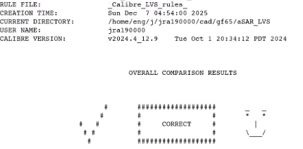
Designed and laid out a 16-bit successive approximation register (SAR) ADC controller on GlobalFoundries 65nm process. The controller implements a binary search algorithm to resolve each bit sequentially — evaluating the MSB first, then retaining or clearing each bit based on the comparator output until the LSB is resolved. The design supports multi-channel pipeline control for increased throughput and is built for scalability across additional SAR channels. The final layout uses 3,200 custom cells, passes full DRC and Calibre LVS verification.
Design Approach
The primary design constraint was minimizing cell height to maximize the number of channels that fit within a given area. All standard cells were designed to a target height of 3.38 µm without horizontal poly layers for connections — a tight constraint that drove every layout decision. The most significant challenge was creating a custom DFF that matched this cell height; without it, every other cell in the library would need to increase in size, inflating the overall footprint. A custom split inverter was introduced to solve a routing conflict within the DFF, enabling the design to maintain its target height while achieving correct rising-edge behavior.
Placement and routing was performed in Innovus. Pin widths were tuned to 0.14 µm to resolve
DRC violations near pin centers, and PR boundary rules were manually set during abstract
generation to ensure correct cell fit. LVS setup required careful matching of bus pin naming
conventions (e.g. DACOUT[0:13] referenced as DACOUT<1> in
layout) before the comparison passed cleanly.
Custom DFF Cell Design
A custom D flip-flop was designed from scratch on GF 65nm to serve as the register element within the SAR controller. The design goal was to match the 3.38 µm cell height of the rest of the standard cell library. No horizontal Metal 2 was used; all routing was accomplished on Metal 1 with Metal 2 reserved for pins only. Pin pitch is 0.26 µm with JX/JZ borders at n × 0.26 µm + 0.13 µm.
An original architecture mistake caused the DFF to trigger on a falling edge. The fix required introducing a split inverter — a novel layout variant that allows three Metal 1 wires to bypass a gate, which was otherwise impossible at this cell height. The split inverter was independently DRC, LVS, and HSPICE verified before integration.
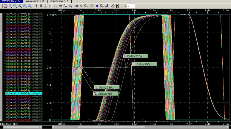
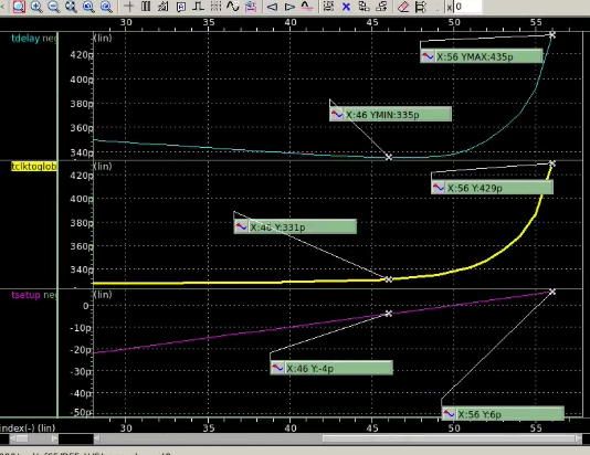
DFF Measurements
| Parameter | Transition (0→1) | Transition (1→0) |
|---|---|---|
| Tsu_DD (setup, drop-dead) | 25 ps | 6 ps |
| Tsu_opt (setup, optimal) | 41 ps | 4 ps |
| Thold | 6 ps | 25 ps |
| TCLK→Q (optimal) | 329 ps | 331 ps |
| tD (D→Q, optimal) | 370 ps | 335 ps |
| Cell Height | 3.38 µm | |
| Cell Width | 11.7 µm | |
| Cell Area | 39.546 µm² | |
DFF Analysis Report
Full layout walkthrough, split inverter design, setup/hold time characterization, and HSPICE verification.
Open DFF Analysis in New TabLayout & Verification
Full SAR Project Report
Includes testbench Verilog results, cell count, routing report, DRC and LVS verification.
Open Full Report in New Tab