7nm 128b S2P & Custom Cell Library
Spring 2026
Overview
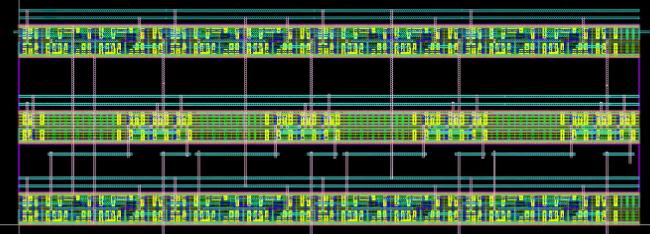
Built a 128-bit serial-to-parallel (S2P) converter entirely from a custom standard cell library on the ASAP7 7nm FinFET PDK, done as a feasibility project for EECT/CE 7325 VLSI Design. Every cell — inverter, NAND2, NOR2, and a custom negative-edge DFF — was designed by hand, and the full 128-bit design was manually placed and routed rather than run through an automated PnR flow. The final design passes DRC and LVS clean at 685 cells in a 23×23 µm footprint. The project was graded competitively on cell count under manual PnR, which shaped most of the architectural decisions below.
Custom Cell Library
Four base cells were designed from scratch on ASAP7, each independently verified for DRC, LVS, and waveform correctness under a 15fF load with 12 ps input slew (0–100% and 100–0%).
Cell Dimensions & Area
| Cell | Dimensions (µm) | Area (µm²) |
|---|---|---|
| INV | 0.288 × 0.162 | 0.046656 |
| NAND2 | 0.216 × 0.288 | 0.062208 |
| NOR2 | 0.216 × 0.288 | 0.062208 |
| DFF (neg-edge) | 1.35 × 0.288 | 0.388 |
The DFF is a negative-edge flip-flop with three diffusion breaks. In hindsight, flipping the
first latch stage horizontally would have eliminated one of them — a DRC rule around active
region margins for excised gates wasn't fully accounted for until after the cell was
finished. The library's .lib/.db characterization files were built
from these four cells and used directly for synthesis and LVS matching throughout the
project.
Architecture & Design Approach
An S2P converter takes a serial bitstream — one bit shifted in per clock cycle — and presents it as a parallel word once a full frame has been received. Since PnR was entirely manual, the priority was partitioning the design into reproducible, independently verifiable blocks rather than one monolithic layout:
- DFF shift chain — the register chain the serial bits propagate into.
- Binary counter — counts DFF transitions to know when a full word has loaded.
- Valid/enable logic — small NAND+INV gating that flags a completed frame.
- Output register — captures the shift chain into the parallel output on sync, built from NAND-gated registers.
A 4-bit prototype was built and verified first to validate the partitioning before scaling to 128 bits — the DFF chain and output register both scale linearly and reuse the same routing pattern per bit, so once 2 bits passed LVS cleanly, scaling to 4, then 128, was mostly repetition.
Building a Counter Without a Native XOR Cell
Counting to 128 requires a 7-bit binary counter, and a ripple/binary counter's carry logic is naturally XOR-based. The cell library only included NAND2 and INV, so each counter bit was built as a pseudo-XOR from four NAND2s plus an inverter, with each stage's carry term built from an AND chain (NAND2 + INV) over all lower bits:
assign d0 = ~cnt[0];
assign d1 = cnt[1] ^ cnt[0];
assign d2 = cnt[2] ^ (cnt[1] & cnt[0]);
assign d3 = cnt[3] ^ (cnt[2] & cnt[1] & cnt[0]);
assign d4 = cnt[4] ^ (cnt[3] & cnt[2] & cnt[1] & cnt[0]);
assign d5 = cnt[5] ^ (cnt[4] & cnt[3] & cnt[2] & cnt[1] & cnt[0]);
assign d6 = cnt[6] ^ (cnt[5] & cnt[4] & cnt[3] & cnt[2] & cnt[1] & cnt[0]);
Each AND term reuses the previous stage's output rather than re-deriving it, so the AND chain could just be extended by one NAND2+INV pair per bit and copied down the counter. The pseudo-XOR gate turned out to be the most LVS-fragile block in the whole design — it's extremely sensitive to naming and wiring at the schematic level, and it took the most iteration to get matching cleanly against layout. A synthesis library mismatch (positive-edge DFF assumed by the synthesized netlist, versus the actual negative-edge custom DFF) also surfaced during this stage and required re-deriving the affected module logic once corrected.
Verification & Results
The final 128-bit design passes DRC and LVS clean at 685 cells total in a 23×23 µm footprint. Since the project was scored competitively on cell count under manual PnR rather than timing or power, fanout optimization was deliberately left out — parasitics and timing were expected to (and did) suffer as a tradeoff for cell-count efficiency.
Functional verification used a reduced 4-bit testbench for waveform readability (the full
128-bit structural Verilog, layout, schematics, and HSPICE scripts are included in the
report below). The simulation shifts in a 128-bit serial message, confirms the first 15
MSBs against an expected pattern (101100101110101), and validates the
valid-out/counter interaction against the parallel output register — all cross-checked
against a full reset sanity test.
As a stretch goal, a 9-channel 128-bit S2P was also architected at the hierarchical schematic level, scaling to roughly 6,165 cells — though it wasn't simulated due to workstation constraints, and manually renaming 128 parallel-output ports per channel wasn't worth pursuing by hand.
Full S2P Project Report
Complete design walkthrough, module-by-module schematics, DRC/LVS verification, and simulation waveforms.
Open Full Report in New Tab